Call us now :08045803043

 Send Inquiry
PCB Design And Development
Price 500.0 INR/ Number
PCB Design And Development Specification
- Impedance
- Controlled, as per request
- Silkscreen
- White
- Test
- Other
- Min. Line Width
- 0.152 mm (6 mil)
- Hole Size
- 0.3 mm
- Insulation Resistance
- >10^12
- Voltage Endurance
- 2 kV
- Soldermask
- Green
- Board Type
- Rigid
- Min. Line Spacing
- 0.152 mm (6 mil)
- Flame Resistance Level
- UL94V-0
- Product Type
- PCB Design And Development
- Base Material
- Other
- Surface Finish
- HASL
- Copper Thickness
- 35 microns
- Board Thickness
- 1.6 mm
- Color
- Green
- Panel Size
- 457 x 610 mm
- Sensor Switch
- No
- Electrical Components
- As per design
- Number Of Layers
- 2
- Design File Support
- Gerber, DXF, ODB++
- Assembly Service
- Available
- Customization
- Supported (Prototype to Mass Production)
- RoHS Compliant
- Yes
- Component Placement Accuracy
- 0.1 mm
- Operating Temperature Range
- -40C to +130C
PCB Design And Development Trade Information
- Minimum Order Quantity
- 10 Number
- Payment Terms
- Cash in Advance (CID)
- Supply Ability
- 5000 Per Month
- Delivery Time
- 10 Days
- Main Domestic Market
- All India
About PCB Design And Development
What is PCB ?
A Printed Circuit Board (PCB) is a flat board used to mechanically support and electrically connect electronic components using conductive copper tracks. It serves as the foundation of most electronic devices, allowing components like resistors, capacitors, and integrated circuits to work together efficiently. PCBs help improve reliability, reduce wiring complexity, and ensure compact, organized, and high-performance electronic systems.
Benefits of PCB Design & Development
- Custom PCB Design: The creation of PCBs tailored to specific application needs, ensuring optimal performance, reliability, and efficient integration into electronic systems.
- Schematic Capture & Simulation: Involves creating accurate circuit diagrams and testing their behavior virtually before PCB layout. This process helps identify errors early, verify performance, and ensure reliable and efficient circuit operation.
- PCB Layout & Routing: Involves placing components and designing copper traces to ensure proper signal flow, minimal interference, and efficient thermal management for reliable circuit performance.
- Prototyping & Fabrication: Involve converting the final PCB design into a physical board for testing and validation. This stage ensures the design performs as expected before moving into full-scale production.
- Testing & Validation: Ensures the PCB functions correctly and reliably by checking performance and detecting defects before final production.
Introducing our Trending PCB Design and Development solutions, featured for their commanding performance and enviable reliability. With an optimum operating temperature range from -40C to +130C and precise component placement accuracy of 0.1 mm, each panel is tailored for both prototype and mass production. Our RoHS-compliant boards come with complete assembly services and support all major design file formats, ensuring versatility. Grab yours with confidence-customization options, stringent electrical testing, and a durable finish guarantee dependable results for distributors, manufacturers, service providers, suppliers, and traders across India.
Leading Features and Applications of PCB Design and Development
Our PCB Design and Development services deliver rigid, two-layer boards with controlled impedance, high insulation resistance, and HASL surface finish. Engineered for outstanding performance in electronics, automation, and industrial control systems, these PCBs are ideal wherever precision and durability are required. Designed for seamless integration, simply provide your design files-Gerber, DXF, or ODB++-and specify your assembly needs. Boards are ready to use after 100% electrical testing, offering you peace of mind and streamlined deployment.
Certifications, Supply Chain, and Export Details of PCBs
Each PCB boasts UL94V-0 flame resistance and RoHS compliance, guaranteeing safety and environmental governance. With a robust supply ability to handle diverse scale requirements, orders are efficiently dispatched in secure packaging at a competitive list price. Our products are regularly exported to main markets worldwide, testament to enduring global trust. Clients benefit from reliable delivery timelines, quality-assured packaging standards, and consistent support throughout the procurement process.
FAQ's of PCB Design And Development:
Q: How do I start the process of ordering a customized PCB?
A: To begin your order, submit your design files (Gerber, DXF, or ODB++) and specific requirements. Our team will review your project and guide you through prototyping or mass production with assembly service options.Q: What is the benefit of the 0.1 mm component placement accuracy?
A: The 0.1 mm placement accuracy ensures precise, error-free assembly of electrical components, enhancing the reliability and performance of your finalized boards.Q: When are the PCBs typically dispatched after the order?
A: PCBs are dispatched promptly after completion of electrical testing and assembly. Exact timelines depend on your customization and quantity specifications-our team ensures timely and reliable shipping.Q: Where can these PCBs be used?
A: These PCBs are suited for use in electronics manufacturing, industrial control systems, automation equipment, and various other command-level applications requiring robust and precise board solutions.Q: How does RoHS compliance benefit my projects?
A: RoHS compliance means your projects conform to environmental regulations, reduce hazardous substances, and meet green manufacturing standards-important for both safety and market acceptance.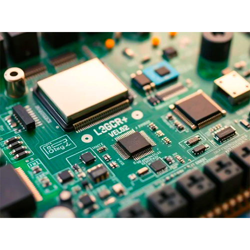
Tell us about your requirement

Price:
Quantity
Select Unit
- 50
- 100
- 200
- 250
- 500
- 1000+
Additional detail
Mobile number
Email

Our Products
- ABB Brand
- Programmable Logic Controller (PLC)
- Human Machine Interface (HMI)
- AC Drives (VFD)
- Servo Motor And Drives
- Industrial Drives
- Teltonika Brand
- 4G - 5G Cellular Router
- Industrial Ethernet Switches
- Industrial Rugged Gateways
- WiFi Access Point
- Remote Management System (RMS)
- GreenFuturz RFID
- RFID Reader And Antenna
- RFID Tags
- RFID PRINTER
- RFID Self Checkout
- RFID Tunnel Reader
- RFID Smart Shelf - Cabinet
- Posital Fraba
- Incremental Encoder
- Absolute Encoder
- Linear Sensor
- Digital Inclinometer
- Lifo Brand
- PCB Design And Development
- Industrial Router
- IOT Gateway
- Din Rail Switch
- Automation Components
- Servo Drive


G-123, Sector-63,Noida - 201307, Uttar Pradesh, India

Mr. Amit Kr. Singh
(Proprietor)
Mobile :08045803043
 Send Inquiry
 Send SMS
 Call Me Free
Developed and Managed by Infocom Network Private Limited.
